X-ray Scattering and Spectroscopy
Research at LAS concentrates on the characterisation of thin films, interfaces and nanostructures using X-ray scattering techniques. Such materials play an important role in modern technology – layers of only a few nanometers thickness form the basis of state-of-the-art high-density integrated chip fabrication, while thin films of materials such as carbides or nitrides, with thicknesses of only several 10s of nanometers, provide corrosion and temperature resistance for mechanical structures such as aircraft turbine blades.
Of special interest is the elucidation of nanoscale structural information during materials processing, for example:
- in situ observation of structure formation during growth processes
- operando analysis of material processing/cycling
- multi-scale resolution (atomic to nanoscale, correlation to macroscale) and methodical combination
For the characterisation of such materials LAS employs a range of experimental synchrotron-based methods such as:
- High-resolution X-ray diffraction (HRXRD)
- X-ray Reflection (XRR)
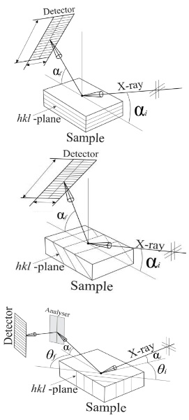
- Grazing-incidence small-angle scattering (GISAXS)
- Grazing incidence X-ray diffraction (GID)
- Reciprocal Space Mapping
both at the KIT Synchrotron source and at other leading synchrotron sources.
|
|
|
|
Typical scattering geometries for the characterisation of thin films, interfaces and nanostructures |
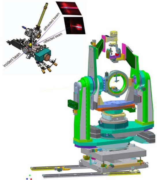
The heavy-duty diffractometer at the NANO beamline at the KIT-Synchrotron is specifically designed for in-situ structure characterisation of nanoscale materials.
|
|
Example: structure influence on dynamics and related physical properties of thin films and nanostructures
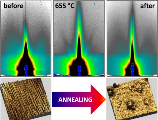
The thermal stability of parallel, high aspect ratio DySi2 nanowires and nanoislands self-organized on vicinal Si(001) is investigated as a function of the annealing temperature from room temperature up to 760 °C by in situ grazing incidence small-angle X-ray scattering (GISAXS). A transformation of the nanoobjects has been observed above a temperature of 500 °C. The nanowires collapse forming small islands, while the nanoislands grow in size due to Ostwald ripening. The formation of facets is observed during annealing. Combining the in situ GISAXS experiment with atomic force microscopy measurements leads to a comprehensive understanding of the observed surface morphology changes. |
|
|
|
|
A. Seiler, S. Ibrahimkutty, P. Wochner, R. Pradip, O. Waller, et al., Thermal Stability Studies of DySi2 Nanowires and Nanoislands by In Situ GISAXS, J. Phys. Chem. C 120 (2016) 7365 – 7372.
Example: Application of asymmetric skew X-ray diffraction to semiconductor nano-objects
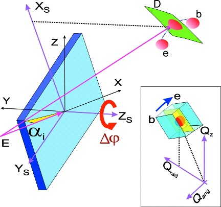
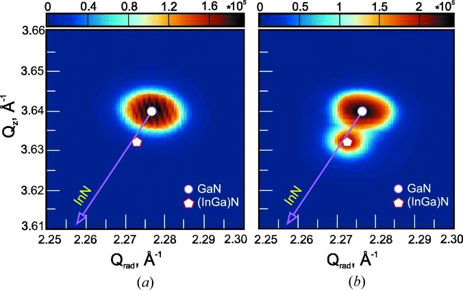
Procedures for obtaining three-dimensionally resolved reciprocal-space maps in skew X-ray diffraction geometry allow tuning of the information depth in the range from tens of micrometres for symmetric skew diffraction down to tens of nanometres for strongly asymmetric skew geometries, where the angle of incidence is below the critical angle of total external reflection.
|
|
|
|
A scheme of the scan in the laboratory coordinate system is shown. The green surface marked with D corresponds to the segment of the Ewald sphere covered by the detector window. The scan is executed by a rotation about the zS axis (Δφ). |
Qrad–Qz intensity maps for the reflection with incident angles of (a) 10° and (b) 0.3°. The positions of GaN and low-In QDs in reciprocal space are marked by circles and pentagons, respectively. Arrows point to the InN reciprocal node (relaxation direction), which deviates slightly from the direction to the coordinate origin. |
|
D. Grigoriev, S. Lazarev, P. Schroth, A. Minkevich, M. Köhl, T. Slobodskyy, M. Helfrich, D. M. Schaadt, T. Aschenbrenner, D. Hommel and T. Baumbach (2016). J. Appl. Cryst. 49, 961-967 https://doi.org/10.1107/S1600576716006385 |
|

